High-throughput Fabrication and Characterization of TFTs
Yanbing Han1, Qun Zhang2*
1 Zhengzhou University, Zhengzhou, 450052, China
2 Fudan University, Shanghai, 200433, China
EXTENDED ABSTRACT: High-throughput theory and method have been developed in recent years, which can help to investigate the physical optoelectronic properties of materials as a function of their compositions and structures efficiently. Most reports only focus on the non-gas elemental compositions. For example, in the investigation of p-type wide band gap semiconductor BaCu2S2, the optoelectronic properties as a function of Ba/Cu ratio can be studied conveniently by co-sputtering from BaS and CuS targets. However, gas elements play an important role in some other research fields, like the oxygen content has strong influences on performances of the thin film transistors. Unfortunately, there is lack of knowledge on how to introduce the gas element gradient into the high throughput method.
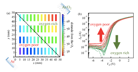
This work proves that gas content can be successfully introduced as a variation in the high throughput fabrication of thin films and thin film transistors by specially design technique. Two identical targets was utilized for co-sputtering, but provided with/without nitrogen. The characterization results show that nitrogen gradient was achieved in thin films[1]. Base on this result, IZO thin film transistors were also fabricated with the similar technique. The performances of thin film transistors were closely related with the oxygen, proving the high throughput gas content was realized in thin film transistors[2]. The experimental results above can facilitate the application of gas content into the high throughput fabrication of thin films and electronic devices.

Figure 1. Schematic of thin films with high throughput oxygen gradient and the performances of related TFTs
REFERENCES
[1] ACS Comb. Sci. 2018, 20, 436−442; [2] Chin. Phys. B Vol. 29, No. 1 (2020) 018502

Yanbing Han has completed his PhD from Fudan University, during which he studied in NREL as visiting scholar for two years. Currently, he works in Zhengzhou University. He has long worked on the synthesize and characterization of chalcogenide thin films and related electronic devices, and has published more than 20 papers on journals like 《Chemical Reviews》, 《Chemistry of Materials》, 《Physical Review Applied》. Now he is a principal investigator on projects from National Science Foundation of China, et al.